High throughput on-chip analysis of high-energy charged particle tracks using lensfree imaging (2015)
W. Luo, F. Shabbir,

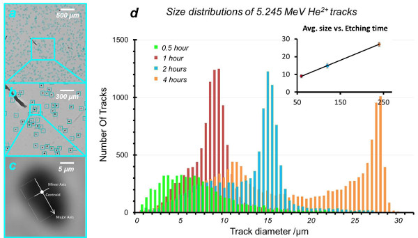
We demonstrate a high-throughput charged particle analysis platform, which is based on lensfree on-chip microscopy for rapid ion track analysis using allyl diglycol carbonate, i.e., CR-39 plastic polymer as the sensing medium. By adopting a wide-area opto-electronic image sensor together with a source-shifting based pixel super-resolution technique, a large CR-39 sample volume (i.e., 4 cm × 4 cm × 0.1 cm) can be imaged in less than 1 min using a compact lensfree on-chip microscope, which detects partially coherent in-line holograms of the ion tracks recorded within the CR-39 detector. After the image capture, using highly parallelized reconstruction and ion track analysis algorithms running on graphics processing units, we reconstruct and analyze the entire volume of a CR-39 detector within ∼1.5 min. This significant reduction in the entire imaging and ion track analysis time not only increases our throughput but also allows us to perform time-resolved analysis of the etching process to monitor and optimize the growth of ion tracks during etching. This computational lensfree imaging platform can provide a much higher throughput and more cost-effective alternative to traditional lens-based scanning optical microscopes for ion track analysis using CR-39 and other passive high energy particle detectors.
Detection of charged particles, especially ions such as alpha particles or protons, has been of interest to the scientific community, driven by various fields such as radiotherapy, medicine, accelerator research, and environmental monitoring.1–10 Being a passive detector, allyl diglycol carbonate polymer, i.e., CR-39, is one of the gold standard materials for charged particle detection.1–4,11,12 Despite its major advantages such as a large sensing area with sensitivity to single particles such as protons and excellent immunity from electromagnetic pulses and x-rays, the broad adoption of CR-39 detectors is hindered by the laborious analysis procedures that involve conventional lens-based scanning optical microscopy. The standard analysis starts with batched chemical etching of a number of CR-39 detectors of interest, all in parallel, for 1–4 h to convert the ion induced damage of the chemical bonds into pits and then involves using scanning optical microscopy to inspect both surfaces of the detector, each up to a depth of ∼150 μm. Under the same etching conditions, the penetration depth resolved in CR-39 detectors is proportional to the initial kinetic energy of the accelerated particles. Due to its limited field-of-view (FOV), a lens-based optical microscope has to mechanically scan across the exposed area (e.g., ∼16 cm2), which typically takes several minutes for each detector sample. Various applications including accelerator diagnosis8 and environmental monitoring using CR-39 detectors can generate large amounts of samples to be analyzed, making this optical inspection step a significant bottleneck due to its lengthy and laborious process.
Here, we demonstrate that lensfree on-chip microscopy can provide a high-throughput alternative to conventional lens-based scanning microscopes to enable rapid imaging and automated analysis of ion tracks that are recorded using CR-39 detectors. As shown in Fig. 1, our lensfree microscopy set-up features an ultra-wide FOV of ∼18 cm2 which is enabled by its wide-area CCD chip (Kodak KAF39000, 39.0 megapixels, 49.0 mm × 36.8 mm active area, pixel pitch 6.8 μm) and unit magnification on-chip imaging geometry, where the CR-39 sample of interest is directly positioned on the CCD chip with a vertical distance of ∼1.5 mm to its active area. In this lensfree imaging setup, a partially coherent light source (Fianium Whitelase, 530 nm central wavelength, ∼2.5 nm spectral bandwidth) is coupled into a single mode fiber, which is vertically mounted ∼30 cm above the center of the image sensor chip. This illumination light from the fiber tip first impinges on the sample, typically a 4 cm × 4 cm CR-39 plastic plate, and the holographic diffraction patterns caused by the etched ion tracks are directly captured by the CCD image sensor. Then, the optical fiber tip above the sample plane is laterally shifted by a two-axis automated mechanical stage to generate sub-pixel shifted holograms on the image sensor plane. These sub-pixel shifted in-line holograms are digitally fused together to synthesize high resolution images of the sample through a pixel super-resolution algorithm, which resolves the holographic fringes that are normally under-sampled by the native pixel size of the sensor-array.13–18 By capturing 16 different sub-pixel shifted holograms via source-shifting, this lensfree on-chip microscopy setup can probe the entire CR-39 sample volume over a large FOV of ∼18 cm2 with an effective numerical aperture (NA) of ∼0.1 in less than 1 min. After this image capture step, using a parallel computing platform involving two NVIDIA K20C Tesla graphics processing units (GPUs) with compute unified device architecture (CUDA), the reconstruction and ion track analysis of our large sample FOV (18 cm2) can be completed within ∼1.5 min.